Jun 04 2019.
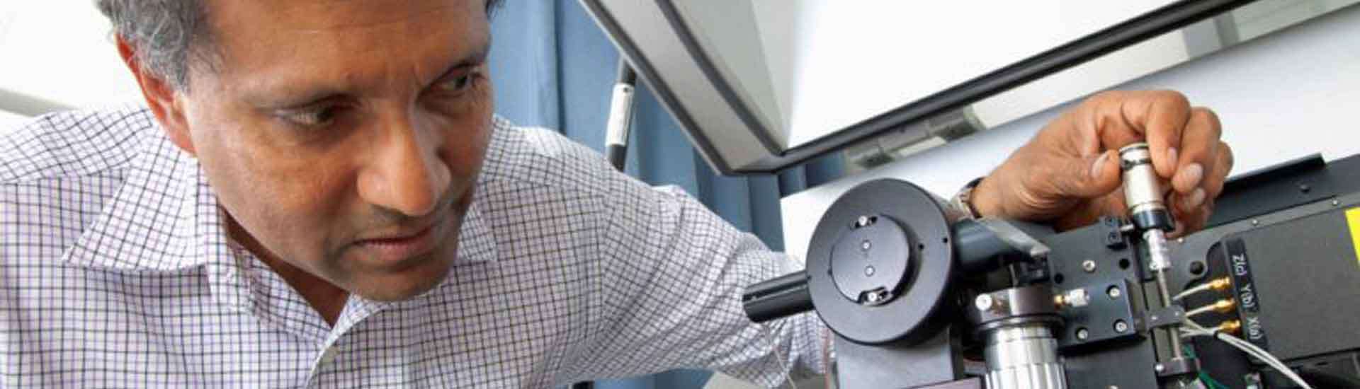
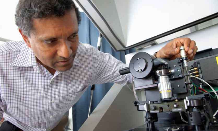
views 418Sometimes, little things take up a lot of space in your life. As for Prof. Hemantha Kumar Wickramasinghe,a greater part of his life was spent studying and researching on micro and nano materials. Having had his primary education at Royal College, Colombo, he obtained a B.Sc and a PhD in Electrical Engineering from the University of London. After several placements in his academic career, in 1984 he joined IBM. It was here that he led the team that developed atomic force microscopes and went on to invent a number of novel scanning probe microscopes and even applied them to data storage and various other requirements. With over 100 patents for his innovations, Prof. Wickramasinghe has earned various awards and accolades for his dedication towards the fields of nanotechnology and microscopy.
Currently, Wickramasinghe, a Distinguished Professor at the University of California, Irvine (UCI) holds joint appointments in UCI’s Biomedical Engineering, Materials Science and Engineering Departments. He is also the Nicolaos G. & Sue Curtis Alexopoulos Presidential Chair in Electrical Engineering and Computer Science. Lately, he has been working on instruments to improve the understanding of biological processes and enable rapid, point-of-care diagnosis of bacterial and viral infections. Amidst his contributions to the two fields, Prof. Wickramasinghe was also instrumental in establishing the Sri Lanka Institute of Nanotechnology. In recognition of his contributions for Improving Natural Knowledge, Prof. Wickramasinghe will be inducted as a Fellow of the Royal Society of London this July. While fellows are elected for life, his name will now be read alongside influential physicists including Isaac Newton, Christopher Wren, Charles Darwin and Stephen Hawking.
In an interesting conversation with the Daily Mirror Life, Prof. Wickramasinghe shared his experiences in the fields of nanotechnology and microscopy, challenges he faced andthe most satisfying part about his career.
Q: What inspired you to get involved in the field of nanotechnology?
A: Nanotechnology as a field did not exist when I started working on building advanced, ultra high magnification microscopes. Shortly after I joined IBM in the mid 1980s, I spent the first six months visiting all the manufacturing and development lines at IBM. I discovered during those visits that all the critical measurements for quality control (such as line width control of silicon circuits) in their production lines were done by hundreds of operators looking through standard optical microscopes! It was clear to me, based on Moor’s law scaling, that we would need some new way to measure and control the manufacturing process once feature sizes shrunk below the optical microscope resolution limit – i.e around 0.5 micro meters. I got involved with nanotechnology to try and replace those optical microscopes with something more powerful and better.
Q: Back then when you started studying the field, what challenges did you have?
A: There were several challenges. I will just mention a few high level ones. After inventing and demonstrating the non-contact or vibrating mode Atomic Force Microscope (AFM) - a microscope way more powerful thanany optical microscope - I wanted to develop the technology toward aninstrument that could inspect silicon wafers in manufacturing lines. I had great difficulty convincing the “guru’s” at IBM at the time that this was a viable proposition.As a result, I did not get funding on my first try. Finally, with help from my manager Tom Di Stefano, we were able to convince a corporate entity -named IBM Advanced Engineering For Manufacturing which was involved with funding high risk ventures to support the effort. The other major challenge was to convince the customers – the manufacturing line managers – that these new instruments could replace the optical microscopes they were using.
Q: What was your first research project in nanotechnology?
A: My first research project was to build a non-contact scanning thermal microscope (SThM) –a fine needle-like probe (or tip) that could be stabilized at nanometer distances over a sample by measuring and controlling the heat transfer between a heated tip and the sample, and then scanned to record the surface profile. We were able, for the first time, to non -destructively characterize an insulating surface with 30 nanometer resolution. The SThM was a precursor to the AFM we developed.
Q: Your name has been associated with the development of various microscopes. Tell us a bit about them and how the field of microscopy has advanced today.
A: I pioneered the field of Scanning Probe Microscopy (SPM). First, by inventing and developing the vibrating mode AFM and then, based on this platform, creating a range of new scanning probe microscopes. Notable among these is the Magnetic Force Microscope (MFM) used today by all disk drive manufacturers to measure the magnetic performance of disk drives and servers. The SThM is used today to map everything from heat dissipation in high-end microprocessors to nanoscopic thermal property measurements (for example glass transition temperatures) of polymer materials such as paints and pharmaceuticals. The Kelvin Probe Force Microscope (KPFM) is another invention that has found widespread use; it measures nanoscopic changes in work function (the energy required to pull an electron out of a surface). The KPFM is used to study fundamental properties of materials – one example is its use to understand how advanced solar cell materials work. Almost all the SPMs that I invented have today advanced to the point where they can measure these various properties (heat, light, magnetism etc.) down to atomic level.
Q: You have over 100 patents for your innovations. How do you feel when your innovations are used to research on advanced areas in these fields?
A: Whenever I walk into a nanotechnology laboratory in the world and see that the vibrating probe AFM - and all those Scanning Probe Microscopes that I spent many years developing in use, it makes me very happy! The other thing that gives me a thrill, is when I give a talk somewhere and have young students coming running to me saying “So you are Professor Kumar Wickramasinghe –I am pleased to meet you, we studied your paper on the AFM in class” !!
Q: As of late your focus has shifted to developing instruments to study bacterial and viral infections. But people often ignore microbes or even tiny dust particles around them for that matter. Why is this a risk and how should they prepare themselves?
A: Microbes come in many different forms. We have tens of trillions of microbes living in symbiosis with other cells in our body – many of them live in our gut. Some of them help boost our immune system. However, there are others that are harmful and can even cause death. I am focusing on those harmful viruses and bacteria. Some of the harmful bacteria are developing immunity to today’s antibiotics. We need to come up with techniques to rapidly advance the development and testing of new drugs so that we can fight these harmful pathogens.
Q: As an adviser of the Sri Lanka Institute of Nanotechnology what improvements does Sri Lanka need in establishing itself as a research hub in this field?
A: I was one of the four international scientists that helped launch the Sri Lanka Institute of Nanotechnology led by Professor Ravi Silva and Professor Gehan Amaratunga. I believe that Sri Lanka needs to do what Singapore and South Korea did decades ago. Namely to attract the talented young Sri Lankans who have been successful in technology transfer to come back and inject their experiences and create new nanotech industries for Sri Lanka.
Q: Do you see yourself coming to Sri Lanka and sharing your knowledge and encouraging future aspirants who want to pursue a career in Nanotechnology?
A: I spent part of my sabbatical six years ago at the Sri Lanka Institute of Nanotechnology; it was really too short a time. With my current assignment as Chair of my Department, I have had less time to travel and so have been less engaged. I will have more time when I step down from this assignment.
I am ready to serve the country if called upon to do so.
Q: How did you feel when you were named a Fellow of the Royal Society?
A: I was totally thrilled – I did not expect it at all, although I knew that my accomplishments fully deserved the honour. I also wished that my father -who was a mathematics wrangler at Cambridge - was still alive to hear the news.
Q: What is the most satisfying part about being a researcher in nanotechnology and microscopy?
A: To invent new ways to see the nano- world and to use these inventions to discover new science.
Q: What project (s) are you currently working on?
A: I am currently working on an invention that can detect disease by identifying the genetic signatures of disease-causing bacteria and viruses within minutes from a droplet of blood or saliva. I am in the process of commercializing this technology.


0 Comments